Author Topic: Building a modern PCB for the AEK/AEKII  (Read 21946 times)

0 Members and 1 Guest are viewing this topic.

Online Findecanor

  • Posts: 5036
  • Location: Koriko
Re: Building a modern PCB for the AEK/AEKII
« Reply #50 on: Thu, 09 May 2019, 10:40:24 »
Hmm... Something I have not noticed or reflected on before in my ISO AEKII:
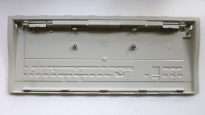
218987-0

The bottom of the case contains moulded depressions for the switch pins on rows B and C. There are also other depressions for jumpers' pins on the PCB. The bottom is thicker around them, but thinner at the bottom row.
I tested with a piece of paper, and found imprints from the pins, so I can confirm that they indeed reach down into these dimples.
This restricts where to put the Alps pins on these two rows: north only.

To fit anything else (such as Cherry MX which also has a centre pin), you would have to make additional dimples with a Dremel.
There is now a choice between losing ISO or flipping Cherry MX upside-down and losing compatibility with silencing clips. I'd vote for the latter because I think there are more ISO users interested in this than people who'd would be interested in dremelling in their case and put Cherry MX with silencing clips on these rows. (Personally, I think MX could be thrown away altogether because there are slider-adapters and Nexus sliders if you want MX keycaps, but no Alps-compatible sliders for Cherry MX that I know of if you are just after the Cherry MX switch feel)

I suppose that the new PCB won't have through-hole diodes or jumpers, but be double-sided with vias and SMD components.
This means that SMD diodes would need to go on the top side or be moved up quite a lot.

It looks like my AEKII case bottom is for both ISO and ANSI. But how is the inside of the AEK case bottom?
« Last Edit: Thu, 09 May 2019, 10:44:00 by Findecanor »

Offline ErgoMacros

  • Posts: 313
  • Location: SF Bay Area
Re: Building a modern PCB for the AEK/AEKII
« Reply #51 on: Thu, 09 May 2019, 11:33:33 »
I don't have my AEK (yet) but here's a photo from the web.  The dimples are there, but so is a stamped metal plate.
Today's quote: '...“but then the customer successfully broke that.”

Offline ErgoMacros

  • Posts: 313
  • Location: SF Bay Area
Re: Building a modern PCB for the AEK/AEKII
« Reply #52 on: Thu, 16 May 2019, 20:38:42 »
 jrfhoutx is working on a similar drop-in replacement for the Apple M0116 and M0118. All components assembled.
   https://geekhack.org/index.php?topic=100749.0;topicseen

Says he wants to do an AEK... some day. (See reddit link)
Maybe some collaboration is in order?

He seems to be farther along. Prototypes out for testing.
Today's quote: '...“but then the customer successfully broke that.”

Offline mythosmann

  • Posts: 24
  • Location: Ohio, USA
  • keyboards aren't even useful
    • My GitHub Page
Re: Building a modern PCB for the AEK/AEKII
« Reply #53 on: Fri, 17 May 2019, 16:48:08 »
jrfhoutx is working on a similar drop-in replacement for the Apple M0116 and M0118. All components assembled.
   https://geekhack.org/index.php?topic=100749.0;topicseen

Says he wants to do an AEK... some day. (See reddit link)
Maybe some collaboration is in order?

He seems to be farther along. Prototypes out for testing.
Yeah, that would be amazing.  It's been a huge oof for me trying to figure out all this stuff.  I ordered some test pcbs with what I figured out about onboard components, and they don't work :(.  I'm still trying to figure it out, but it's not very high on my priority list.  This summer is going to be very hectic, so I don't think this would ever happen if it were just me. 
I'll probably try to get in contact with him, or see if someone else wants to take the wheel.

Offline ErgoMacros

  • Posts: 313
  • Location: SF Bay Area
Re: Building a modern PCB for the AEK/AEKII
« Reply #54 on: Fri, 06 September 2019, 12:56:13 »
OK, Here's another resource (starting point)
   https://github.com/CaninoDev/Mechanical_Keyboard_KiCAD_Templates

KiCAD files for multiple MCUs (ATMega328, ATMega32U4, STM32F072, STM32F303)

14 col x 6 rows, (less 10 blanks) for 74 keys. So we'd need to add 1 more row and 7 more columns. 8 more (28 total) processor pins.
(Looks to me like the STM32F303 has > 30 available IO pins)

Key switch footprints include merged Alps + Cherry MX
Lots of other pointers to resources.

Original announcement here:
  https://geekhack.org/index.php?topic=102332.0;topicseen

Looks like a GREAT place to start!
Today's quote: '...“but then the customer successfully broke that.”

Offline _rubik

  • * Esteemed Elder
  • Posts: 1129
  • Location: 192.168.x.x
  • Typing on: Brutal60, Lavenders Linears, GMK Jamon
Re: Building a modern PCB for the AEK/AEKII
« Reply #55 on: Mon, 09 September 2019, 13:49:45 »
Just had to stop in and express my interest in this project -- will be reading through the repo tonight.

I have a few aek's lying around, and would love to give one a refresh. Thought about starting this project myself, but seems like you have a head start!
ai03 Meridian ¤ Mech 27 ¤ E8.5 ¤ Brutal60 ¤ SSK White Label ¤ HHKB Pro JP ¤ vAEK68 Alps Blues ¤ RF87u

Offline ZyBeR

  • Posts: 178
Re: Building a modern PCB for the AEK/AEKII
« Reply #56 on: Mon, 20 July 2020, 15:29:21 »
Any progress made of late?


Sent from my iPhone using Tapatalk

Offline ebastler

  • Posts: 30
  • Location: Berlin
Re: Building a modern PCB for the AEK/AEKII
« Reply #57 on: Mon, 20 July 2020, 19:14:50 »
Hi, you may find some useful measurments or information in this project: https://github.com/kb-elmo/aek2_usb
Seems to be a drop-in replacement for the AEK2 with QMK support. No clue if it is tested yet.

If you wanna do it SMD, I'd grab an STM32F072. Love those chips and used them in all of my projects so far. Really cheap, jlcpcb assembles them, they have no need for USB series resistors or a crystal for USB and have excellent QMK support.

Good luck with your project!

Offline 4sStylZ

  • Posts: 127
Re: Building a modern PCB for the AEK/AEKII
« Reply #58 on: Mon, 14 September 2020, 04:31:45 »
Now my GF want a full size keyboard so I am also intersted if you finish a drop in replacement pcb for an aek keyboard.

Thank you and good luck.
Bépo user here : AEK64 White linear dampened, XD75 Cherry Blue Jailhoused, TypeMatrix2030 black skin, Lenovo 0B47200 w/ trackpoint, G13, G512. Kensington Expert Trackball & Orbit, Magic touchpad 2.

Offline linuxleah

  • Posts: 95
Re: Building a modern PCB for the AEK/AEKII
« Reply #59 on: Thu, 27 May 2021, 10:45:48 »
I'm in the process of preparing for a production run of Elmo's AEK II USB drop-in replacement PCBs.

If anyone is interested, please see my Interest Check thread at https://geekhack.org/index.php?topic=113053.0