Big progress! I finally got some time to finish routing and I've sent the board off to the fab!

I'll go through some of my routing decisions.
The component side of the board (numpad on the left) board was split up like this:
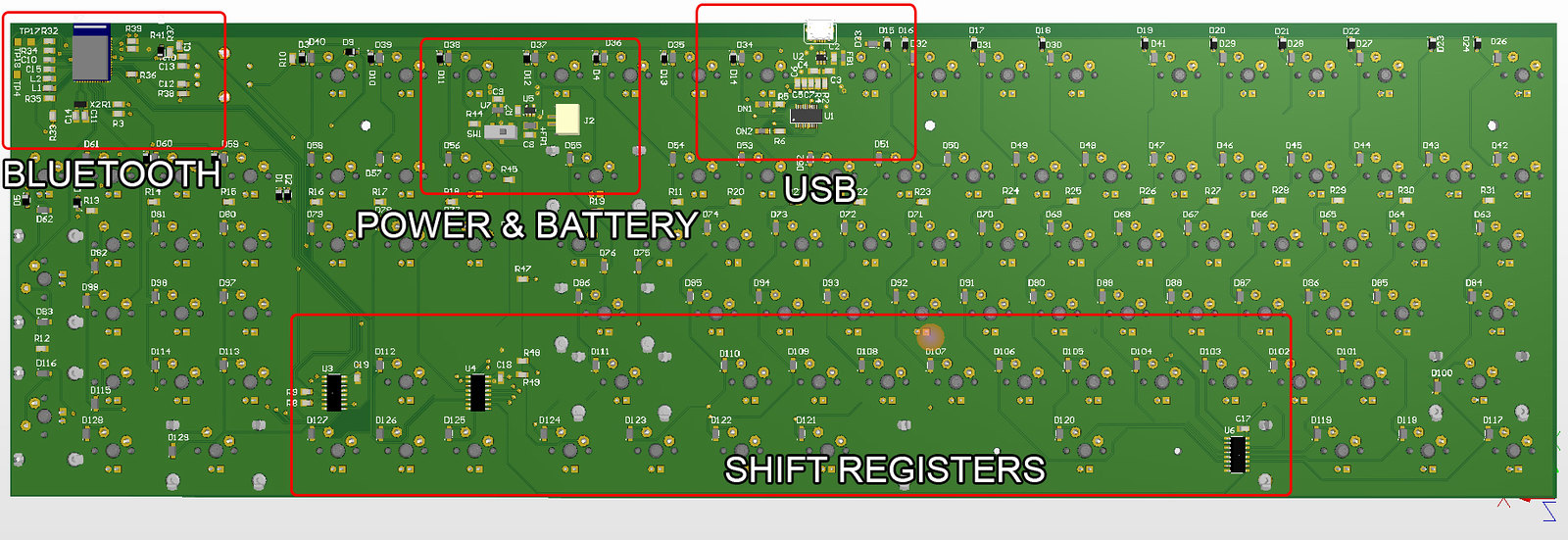
USB signals were routed first since they're really the only high speed thing on the board. I followed the chip vendor's PCB prints here
https://www.ftdichip.com/Support/Documents/PCBData/NerO%20PCB%20Prints.PDF and tried to length match the differential pairs to 5mil. This will definitely be an annoying area to hand solder due to the density of the parts. I chose fairly big footprints for the passives at 0805 packages, so I'm confident it'll come together.

Next came the Bluetooth MCU. The Bluetooth module was placed right on the edge of the board above the numpad. I kept the crystal close to the module, and as far as I could get it from the other signals. The space was pretty constrained, so I ended up killing a bunch of test points in order to make all the parts fit and still leave a ground keepout zone under the antenna. The rotary encoder is mounted just to the right and the signal lines are pretty short. Since the serial lines are really slow, I routed then wherever they fit later in the layout process
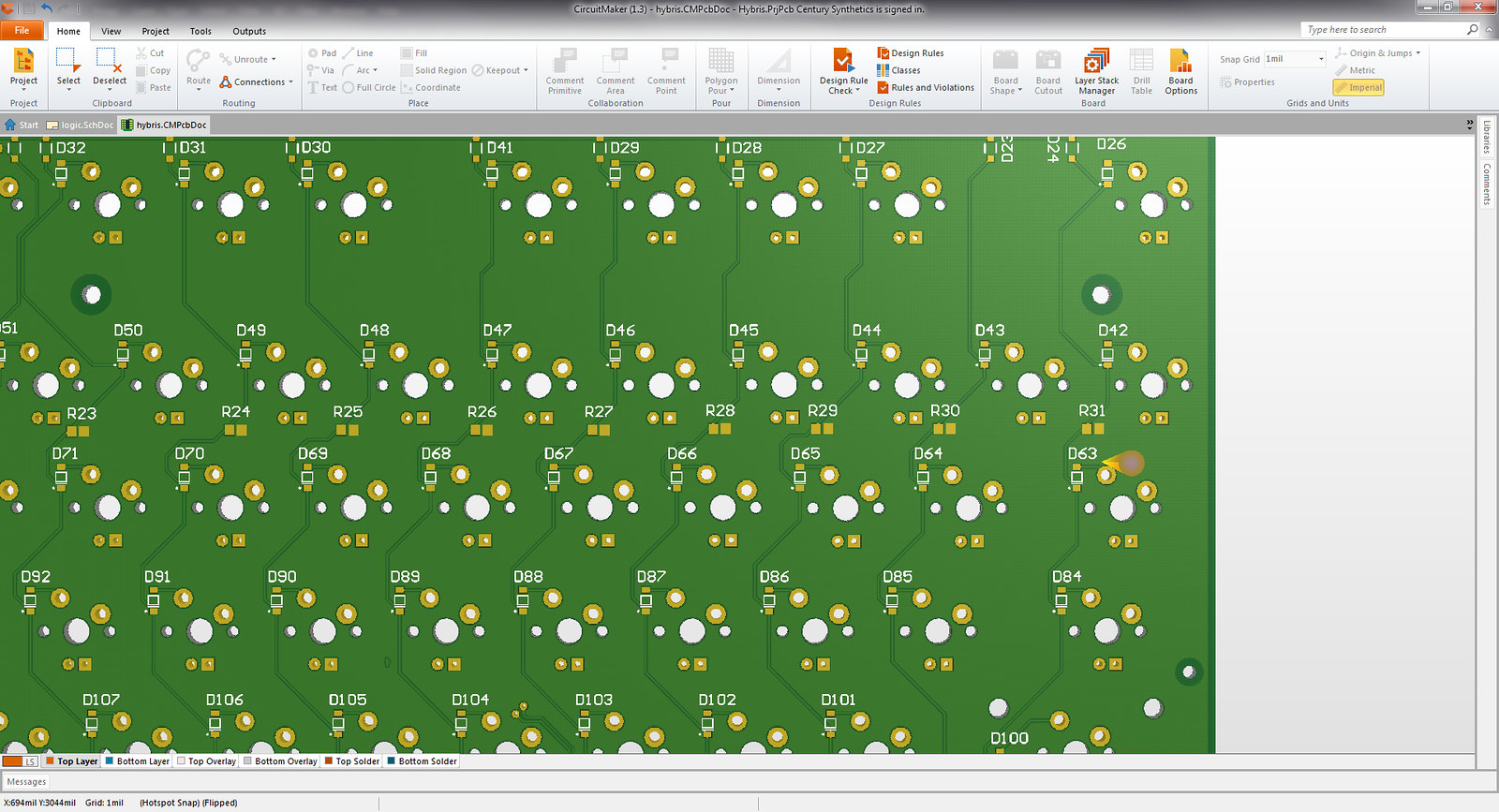
The column layout and diodes were next. I picked a spot and roughly placing the diodes in the same place for most of the 1u switches and did the 1.25/2u ones a little more custom. I'm a little disappointed in the shape of the traces, but this was a good learning experience for what to do better in Rev 2.
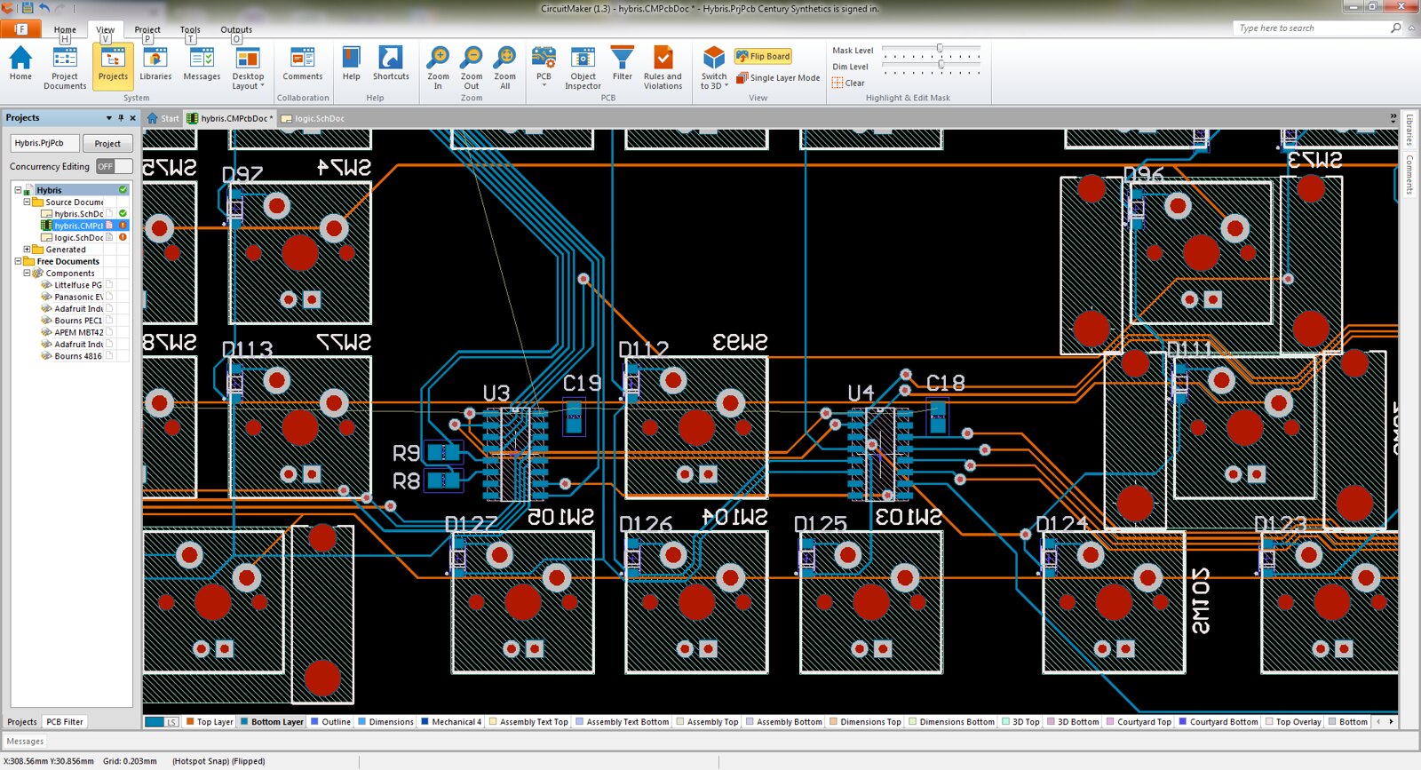
I placed the shift registers next. The data direction ended up being opposite to the breaboard mockup, which ended up making the connection go from the MCU to the register nearest the spacebar. Instead, the data line now goes from the MCU to the register nearest the numpad and daisy chains to the arrow keys then to the spacebar area. I also tried to make the traces not go directly under the stabs, just in case of wear. Any traces routed through the stabs were pulled as close to the mounting holes as possible.
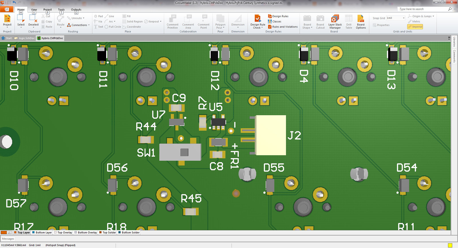
Lastly was the power supply. I was running a little short on space with all of the signal traces, so I picked a convenient spot under the F12 key. Since this will be the highest point of incline, it will let the main board to lay just above the battery inside the case. I'm going to design for a 2000mAh battery, so 60mm x 36mm x 7mm will be the allowance. I've used some fairly beefy traces on the VCC rails just because they have so damn long to go.
I added some more mounting holes to the board after routing all the signals and pulled back the ground plane from all of the holes. That concludes the PCB layout! I'm expecting the boards to arrive as early as tomorrow!
-Rich


