Author Topic: Planck PCB Prototype Build Log  (Read 11545 times)

0 Members and 1 Guest are viewing this topic.

Offline Wilba

  • * Maker
  • Thread Starter
  • Posts: 464
  • Location: Melbourne, Australia
  • Keyboard Stuff Person
    • wilba.tech
Planck PCB Prototype Build Log
« on: Thu, 19 March 2015, 03:38:59 »
Here's my build log of the Planck PCB prototype:


Final shot first, like most build logs.
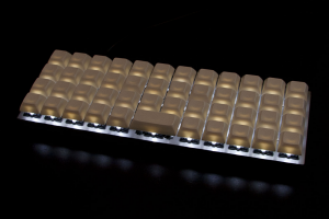
94554-0


Layout a PCB with LEDs on top side of switch. Then throw it away and layout a PCB with LEDs on bottom  side of switch.
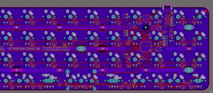
94556-1


Viewing 3D views of the PCB helps catch obvious stuff ups in the silkscreen, and is good for showing you don't use crap like Eagle.
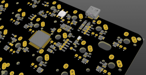
94558-2


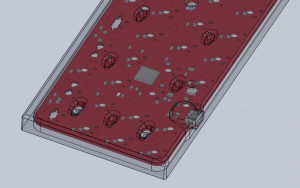
Drag the PCB model into CAD to fit test against existing sheet metal cases and future milled cases. Shown here is a milled case.
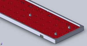
94560-3


Spent a few hours just zooming and rotating, because reasons.
94562-4


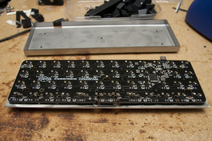
Time to order prototype PCBs. SMD parts soldered with hot air rework station. Switches soldered with my trusty Hakko FX-888. Not the FX-888D. I don't like the D.
94564-5


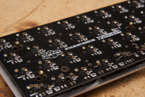
Enhance! Spot the maker's mark in gold. That's gold, Jerry, gold!
94566-6


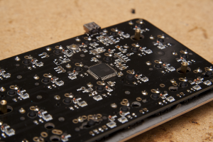
Squeezing an ATmega32U4 between four switches is not for n00bs.
94568-7


Note the LED pads need to be bigger. This is why we prototype.
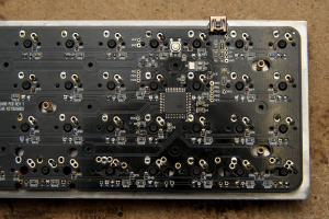
94570-8


Grinding down the bases of stock 3mm round LEDs took longer than soldering the Cherry MX switches. I used SIP socket pins inside the switches so I can swap some 2x3x4 LEDs later.
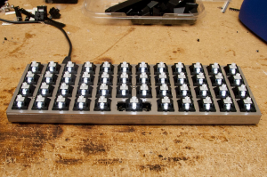
94572-9


LED bling on a keyboard. About as useful as tits on a bull, but OMG IT GLOWZ!!!!!!!!!!11111111111111
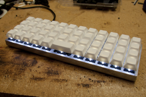
94574-10


« Last Edit: Thu, 19 March 2015, 06:11:10 by Wilba »

Offline regack

  • Posts: 660
  • Location: Thessia
Re: Planck PCB Prototype Build Log
« Reply #1 on: Thu, 19 March 2015, 06:20:04 »
Looks fantastic Wilba!

Offline Nai_Calus

  • * Destiny Supporter
  • Posts: 565
  • Location: Middle of nowhere, CA
  • CLACK
Re: Planck PCB Prototype Build Log
« Reply #2 on: Thu, 19 March 2015, 07:48:31 »
I came.  :-[

Seriously though that is dead sexy. I want a Planck/Atomic but the whole 'hand wiring' thing puts me off when I barely have the confidence to solder a PCB.
- IBM 4704 Model F 107-key "Bertha"
Other boards: Kinesis Essential, Infinity(G.Clears), Ergodox(MX Blues), Monoprice 9433

Eternally searching for Celestial Blue BS V2 and blue/purple Bros.

Offline regack

  • Posts: 660
  • Location: Thessia
Re: Planck PCB Prototype Build Log
« Reply #3 on: Thu, 19 March 2015, 07:56:19 »
I came.  :-[

Seriously though that is dead sexy. I want a Planck/Atomic but the whole 'hand wiring' thing puts me off when I barely have the confidence to solder a PCB.

Honestly, it looks so good, I want to build one just to build it, but I really have no use for it at this point.

I know that OrtholinearKeyboards offers a pre-built version, but maybe you secretly really want to build it yourself?   Really, the hand wiring is more forgiving than the PCB.  Make a mistake, and you can just clip the wires off - you might end up with ugly blobby solder blobs with wire-bits sticking out of them on the bottom of your switches, but it would still work.   

Offline Wilba

  • * Maker
  • Thread Starter
  • Posts: 464
  • Location: Melbourne, Australia
  • Keyboard Stuff Person
    • wilba.tech
Re: Planck PCB Prototype Build Log
« Reply #4 on: Thu, 19 March 2015, 08:06:20 »
I came.  :-[

Seriously though that is dead sexy. I want a Planck/Atomic but the whole 'hand wiring' thing puts me off when I barely have the confidence to solder a PCB.

Honestly, it looks so good, I want to build one just to build it, but I really have no use for it at this point.

I know that OrtholinearKeyboards offers a pre-built version, but maybe you secretly really want to build it yourself?   Really, the hand wiring is more forgiving than the PCB.  Make a mistake, and you can just clip the wires off - you might end up with ugly blobby solder blobs with wire-bits sticking out of them on the bottom of your switches, but it would still work.

The PCB will come with everything soldered except the switches and LEDs. Soldering switches to PCBs is easier than soldering wires... you just snap them all into the plate and they don't move while you use two hands to solder pins to pads. It's a hell of a lot easier than trying to hold a wire to a pin and feed solder while the iron heats both - that requires three hands ;)
« Last Edit: Thu, 19 March 2015, 08:08:21 by Wilba »

Offline jdcarpe

  • * Curator
  • Posts: 8852
  • Location: Odessa, TX
  • Live long, and prosper.
Re: Planck PCB Prototype Build Log
« Reply #5 on: Thu, 19 March 2015, 08:09:33 »
Awesome build, Wilba! :thumb:
KMAC :: LZ-GH :: WASD CODE :: WASD v2 :: GH60 :: Alps64 :: JD45 :: IBM Model M :: IBM 4704 "Pingmaster"

http://jd40.info :: http://jd45.info


in memoriam

"When I was a kid, I used to take things apart and never put them back together."

Offline regack

  • Posts: 660
  • Location: Thessia
Re: Planck PCB Prototype Build Log
« Reply #6 on: Thu, 19 March 2015, 08:44:31 »
I came.  :-[

Seriously though that is dead sexy. I want a Planck/Atomic but the whole 'hand wiring' thing puts me off when I barely have the confidence to solder a PCB.

Honestly, it looks so good, I want to build one just to build it, but I really have no use for it at this point.

I know that OrtholinearKeyboards offers a pre-built version, but maybe you secretly really want to build it yourself?   Really, the hand wiring is more forgiving than the PCB.  Make a mistake, and you can just clip the wires off - you might end up with ugly blobby solder blobs with wire-bits sticking out of them on the bottom of your switches, but it would still work.

The PCB will come with everything soldered except the switches and LEDs. Soldering switches to PCBs is easier than soldering wires... you just snap them all into the plate and they don't move while you use two hands to solder pins to pads. It's a hell of a lot easier than trying to hold a wire to a pin and feed solder while the iron heats both - that requires three hands ;)


Ooh, yes, that would make it really easy.  I was thinking people would be doing the SMD soldering, so this kit would indeed be easier than hand-wiring.  :thumb:

Offline Wilba

  • * Maker
  • Thread Starter
  • Posts: 464
  • Location: Melbourne, Australia
  • Keyboard Stuff Person
    • wilba.tech
Re: Planck PCB Prototype Build Log
« Reply #7 on: Thu, 19 March 2015, 09:06:32 »
The SMD parts are pretty big by modern standards (SOIC, SOT23, 0805) and easy (for some) to hand-solder even with an iron, but it was designed for SMD assembly at the fab.

Offline sypl

  • Posts: 116
Re: Planck PCB Prototype Build Log
« Reply #8 on: Thu, 19 March 2015, 10:30:11 »
Impressive stuff. How do you do the 3D renders of the PCB? Are you using kicad for pcb design?

Offline Nai_Calus

  • * Destiny Supporter
  • Posts: 565
  • Location: Middle of nowhere, CA
  • CLACK
Re: Planck PCB Prototype Build Log
« Reply #9 on: Thu, 19 March 2015, 15:59:55 »
I know that OrtholinearKeyboards offers a pre-built version, but maybe you secretly really want to build it yourself?   Really, the hand wiring is more forgiving than the PCB.  Make a mistake, and you can just clip the wires off - you might end up with ugly blobby solder blobs with wire-bits sticking out of them on the bottom of your switches, but it would still work.   

I kind of do want to build it myself, mostly because it'd be used primarily as a gaming pad and I'd want ergoclears, which aren't an option for getting one pre-built. Between WASD's awful mid-hand twisting and the stiffness of stock Clears, my Code kills my hand on long gaming sessions, but I love it for typing(I'm not a static home row typer, I float, so the hand motions are totally different). I've got an Infinity with Gateron Clears that I use currently, but WASD is still twisty and that's honestly too light and I prefer tactile switches since I play an action MMO and double tapping isn't an issue but knowing I actually did trigger that power is. (Also I'm one of those whackjobs who like full-size keyboards and consider a number pad essential, so until there's a fullsize ortholinear sadly that's not going to be my full-time keyboard because I use the number pad a lot.)

The PCB will come with everything soldered except the switches and LEDs. Soldering switches to PCBs is easier than soldering wires... you just snap them all into the plate and they don't move while you use two hands to solder pins to pads. It's a hell of a lot easier than trying to hold a wire to a pin and feed solder while the iron heats both - that requires three hands ;)

Yeah, I've done a little bit of soldering(Most of a 60%) and it's not too terrifying, but the whole three hands diodes/wire, switches, and solder thing is gah, even if it is more forgiving since you can't lift pads if there aren't any.
- IBM 4704 Model F 107-key "Bertha"
Other boards: Kinesis Essential, Infinity(G.Clears), Ergodox(MX Blues), Monoprice 9433

Eternally searching for Celestial Blue BS V2 and blue/purple Bros.

Offline Wilba

  • * Maker
  • Thread Starter
  • Posts: 464
  • Location: Melbourne, Australia
  • Keyboard Stuff Person
    • wilba.tech
Re: Planck PCB Prototype Build Log
« Reply #10 on: Thu, 19 March 2015, 17:17:45 »
Impressive stuff. How do you do the 3D renders of the PCB? Are you using kicad for pcb design?

I'm using Altium.

Offline jdcarpe

  • * Curator
  • Posts: 8852
  • Location: Odessa, TX
  • Live long, and prosper.
Re: Planck PCB Prototype Build Log
« Reply #11 on: Thu, 19 March 2015, 17:34:51 »
Impressive stuff. How do you do the 3D renders of the PCB? Are you using kicad for pcb design?

I'm using Altium.

Did you type your post using the Planck PCB prototype? Does everything seem to work so far? Inquiring minds want to know!
KMAC :: LZ-GH :: WASD CODE :: WASD v2 :: GH60 :: Alps64 :: JD45 :: IBM Model M :: IBM 4704 "Pingmaster"

http://jd40.info :: http://jd45.info


in memoriam

"When I was a kid, I used to take things apart and never put them back together."

Offline Wilba

  • * Maker
  • Thread Starter
  • Posts: 464
  • Location: Melbourne, Australia
  • Keyboard Stuff Person
    • wilba.tech
Re: Planck PCB Prototype Build Log
« Reply #12 on: Thu, 19 March 2015, 18:40:23 »
Impressive stuff. How do you do the 3D renders of the PCB? Are you using kicad for pcb design?

I'm using Altium.

Did you type your post using the Planck PCB prototype? Does everything seem to work so far? Inquiring minds want to know!

Yes, though adapting to a 40% layout, matrix layout, blank keys and DSA keycaps with deep dish homing keys all in one go isn't that easy for me. The MX clears on this small a plate/case have a great feel... it feels solid when bottoming out, more solid than my Filco.

It's all working fine. The only changes to the PCB for production will be bigger pads for the LEDs.


« Last Edit: Thu, 19 March 2015, 20:19:29 by Wilba »

Offline sypl

  • Posts: 116
Re: Planck PCB Prototype Build Log
« Reply #13 on: Thu, 19 March 2015, 20:09:16 »
Impressive stuff. How do you do the 3D renders of the PCB? Are you using kicad for pcb design?

I'm using Altium.

Thanks for that. I'm kinda new to pcb design.

Can I ask why you've got breakout pins to unused pins, as well as others like d+, d- on the pcb?
https://geekhack.org/index.php?action=dlattach;topic=70092.0;attach=94558;image

Offline Wilba

  • * Maker
  • Thread Starter
  • Posts: 464
  • Location: Melbourne, Australia
  • Keyboard Stuff Person
    • wilba.tech
Re: Planck PCB Prototype Build Log
« Reply #14 on: Thu, 19 March 2015, 20:25:04 »
Impressive stuff. How do you do the 3D renders of the PCB? Are you using kicad for pcb design?

I'm using Altium.

Thanks for that. I'm kinda new to pcb design.

Can I ask why you've got breakout pins to unused pins, as well as others like d+, d- on the pcb?
https://geekhack.org/index.php?action=dlattach;topic=70092.0;attach=94558;image

Some people may want to add stuff to their Planck, e.g. Bluetooth, USB hub, more LEDs, etc. It's even possible to get a custom plate with extra rows and/or columns and manually wire them.


Offline CPTBadAss

  • Woke up like this
  • Posts: 14365
    • Tactile Zine
Re: Planck PCB Prototype Build Log
« Reply #15 on: Fri, 20 March 2015, 06:08:31 »
Nice build log, thanks for sharing it :). I'm actually surprised I never thought of a sheet metal case. Can you share some thoughts about that? Can you compare it to a milled case?

Offline Wilba

  • * Maker
  • Thread Starter
  • Posts: 464
  • Location: Melbourne, Australia
  • Keyboard Stuff Person
    • wilba.tech
Re: Planck PCB Prototype Build Log
« Reply #16 on: Fri, 20 March 2015, 06:40:24 »
I didn't design the case... all credit for that goes to Jack Humbert, who is selling them as part of Planck/Atomic kits: http://ortholinearkeyboards.com/

The formed case is using 1.5mm stainless steel like the top plate, so it's pretty heavy for something this size. Fully assembled it's 600g. Typing feel is solid. That's all I can say, I can't compare it to milled cases because I don't own any.

I'm also surprised I haven't seen more keyboard cases using formed sheet metal. I've been thinking about designing one, inspired by this:


Offline CPTBadAss

  • Woke up like this
  • Posts: 14365
    • Tactile Zine
Re: Planck PCB Prototype Build Log
« Reply #17 on: Fri, 20 March 2015, 06:43:19 »
Now that I noticed it, I agree with you. Sheet metal is a simple solution for making a metal case.

Offline Moralless

  • Posts: 526
  • Location: Sydney, Australia
Re: Planck PCB Prototype Build Log
« Reply #18 on: Fri, 20 March 2015, 06:49:28 »
Thanks for the awesome build log!

Great job on designing the PCB as well. Just want to ask where you got that PCB made since I've been toying around with some personal PCB designs and would like to get them made sometime.

Offline Wilba

  • * Maker
  • Thread Starter
  • Posts: 464
  • Location: Melbourne, Australia
  • Keyboard Stuff Person
    • wilba.tech
Re: Planck PCB Prototype Build Log
« Reply #19 on: Fri, 20 March 2015, 07:02:05 »
These were made by PCBWay: http://www.pcbway.com/

First time I've used them... the quote for 5pcs was cheaper than other fabs, and so I gave them a try. My only complaint would be that the vias, which should be tented (i.e. fully covered by solder mask) appear not to be fully covered, as if they masked out drill holes from the solder mask layer.

Here's an example of what tented vias should look like:


It doesn't affect functionality of the PCB in any way, it's just an observation that it didn't come out exactly as I designed, but for the price, I don't care. Production with assembly will be done with a different fab anyway.

If your PCB designs are smaller than a keyboard, then I highly recommend OSH Park: https://oshpark.com/
Their prices and service are awesome for small prototypes, at the expense of waiting a bit longer for your design to get put on a panel with other designs and produced.
If you ever see a purple PCB for a DIY project, it's highly likely it was made by OSH Park.

Offline Moralless

  • Posts: 526
  • Location: Sydney, Australia
Re: Planck PCB Prototype Build Log
« Reply #20 on: Fri, 20 March 2015, 07:09:18 »
These were made by PCBWay: http://www.pcbway.com/

First time I've used them... the quote for 5pcs was cheaper than other fabs, and so I gave them a try. My only complaint would be that the vias, which should be tented (i.e. fully covered by solder mask) appear not to be fully covered, as if they masked out drill holes from the solder mask layer.

Here's an example of what tented vias should look like:

Show Image


It doesn't affect functionality of the PCB in any way, it's just an observation that it didn't come out exactly as I designed, but for the price, I don't care. Production with assembly will be done with a different fab anyway.

If your PCB designs are smaller than a keyboard, then I highly recommend OSH Park: https://oshpark.com/
Their prices and service are awesome for small prototypes, at the expense of waiting a bit longer for your design to get put on a panel with other designs and produced.
If you ever see a purple PCB for a DIY project, it's highly likely it was made by OSH Park.

Thanks for the reply. Wow those are pretty cheap, but I was planning to use OSH Park when my design is ready, but I thought you got your PCB made in Australia and was hoping to save some money on international shipping :p

So did you get 5 planck PCBs made, if so am I able to buy 1 off you or are the rest off with jackhumbert?

Offline Wilba

  • * Maker
  • Thread Starter
  • Posts: 464
  • Location: Melbourne, Australia
  • Keyboard Stuff Person
    • wilba.tech
Re: Planck PCB Prototype Build Log
« Reply #21 on: Fri, 20 March 2015, 07:14:45 »
I'll ask Jack, he may not need all of them ;)

Offline regack

  • Posts: 660
  • Location: Thessia
Re: Planck PCB Prototype Build Log
« Reply #22 on: Fri, 20 March 2015, 11:14:05 »
These were made by PCBWay: http://www.pcbway.com/

First time I've used them... the quote for 5pcs was cheaper than other fabs, and so I gave them a try. My only complaint would be that the vias, which should be tented (i.e. fully covered by solder mask) appear not to be fully covered, as if they masked out drill holes from the solder mask layer.

-snip-

If your PCB designs are smaller than a keyboard, then I highly recommend OSH Park: https://oshpark.com/
Their prices and service are awesome for small prototypes, at the expense of waiting a bit longer for your design to get put on a panel with other designs and produced.
If you ever see a purple PCB for a DIY project, it's highly likely it was made by OSH Park.

Thanks for the reply. Wow those are pretty cheap, but I was planning to use OSH Park when my design is ready, but I thought you got your PCB made in Australia and was hoping to save some money on international shipping :p


I sent some things off to http://dirtypcbs.com/ to try it out.  The boards are made in china, and shipped out directly from there for reasonable prices.  I haven't gotten mine yet, because it's even slower than Oshpark, but it's also really really cheap if you can fit in the 5x5cm or 10x10cm "protopack" footprints.   I panelized my testers into the 10x10, so in 2-8 weeks, I'll receive ~10 (yes, approximately, might be 8, might be 12, who knows, it's a mystery) boards with 2 designs per board for $25USD shipped.

Offline radish

  • Posts: 126
Re: Planck PCB Prototype Build Log
« Reply #23 on: Tue, 24 March 2015, 21:52:22 »
what is this? a keyboard for ants?!

LZ CP

Offline skullydazed

  • * Vendor
  • Posts: 307
  • Location: Bay Area, CA
  • Had to turn PM's off. Email info@clueboard.co!
    • Clueboard
Re: Planck PCB Prototype Build Log
« Reply #24 on: Tue, 24 March 2015, 22:48:17 »
I'm pretty excited for these. My hand-wiring kit is still on order (should be getting to jack any day now, and then he'll get it out to me) and I'd love a pcb to go with it.