Author Topic: PCB soldering damage  (Read 25191 times)

0 Members and 1 Guest are viewing this topic.

Offline Input Nirvana

  • Master of the Calculated Risk
  • Thread Starter
  • Posts: 2316
  • Location: Somewhere in the San Francisco Bay area/Best Coast
  • If I tell ya, I'll hafta kill ya
PCB soldering damage
« on: Fri, 05 August 2011, 18:08:06 »
Took apart a laptop with 2 physically broken USB ports. Got replacement ports. Attempted to desolder existing ports with a POS Rat **** iron that seemed to fluctuate temp greatly, and it was lead-free solder which I've never experienced. I used wick but couldn't get enough of the solder out to release the old ports. Tip was new, but didn't wet well, not enough flux. Finally got them out and replaced with new ports but did a poor solder job, and both ports are not working. I may have torn a couple of the soldering pads. This weekend I'm using my new soldering station, with a more appropriate tip and a ton of flux, and will desolder the ****ty soldering, clean it up and inspect.

My question:
If any of the pads a torn or missing, if I do a good solder job and the solder wets through the other side of the board, will it catch the trace in the thru-hole? Is there something else I can do to repair it? I'd take it to someone if the repair was $125.

If I need to, I'll but another mainboard on ebay for $180, but if I can fix it, I would prefer to do that.
Kinesis Advantage cut into 2 halves | RollerMouse Free 2 | Apple Magic Trackpad | Colemak
Evil Screaming Flying Door Monkeys From Hell                     Proudly GeekWhacking since 2009
Things change, things stay the same                                        Thanks much, Smallfry  
I AM THE REAPER . . . BECAUSE I KILL IT
~retired from forum activities 2015~

Offline alaricljs

  • I be WOT'ing all day...
  • ** Moderator Emeritus
  • Posts: 3715
  • Location: NE US
PCB soldering damage
« Reply #1 on: Fri, 05 August 2011, 18:29:03 »
If you really only pulled the pad on one side, the through hole should have copper and be attached to the other pad.  If that's the case you should be able to catch it no problem.
Filco w/ Imsto thick PBT
Ducky 1087XM PCB+Plate, w/ Matias "Quiet Click" spring-swapped w/ XM Greens

Offline Input Nirvana

  • Master of the Calculated Risk
  • Thread Starter
  • Posts: 2316
  • Location: Somewhere in the San Francisco Bay area/Best Coast
  • If I tell ya, I'll hafta kill ya
PCB soldering damage
« Reply #2 on: Fri, 05 August 2011, 18:34:18 »
When I desolder, if there is a pad on at least one side, it's part of the copper lining the thru-hole that the trace would be attached to?
Kinesis Advantage cut into 2 halves | RollerMouse Free 2 | Apple Magic Trackpad | Colemak
Evil Screaming Flying Door Monkeys From Hell                     Proudly GeekWhacking since 2009
Things change, things stay the same                                        Thanks much, Smallfry  
I AM THE REAPER . . . BECAUSE I KILL IT
~retired from forum activities 2015~

Offline bluecar5556

  • Posts: 126
PCB soldering damage
« Reply #3 on: Fri, 05 August 2011, 18:41:00 »
For the sake of blabbing, dip the de-soldering wick in flux, otherwise there will be too much heat build up and the PCB traces will become a heatsink.  Do you have an air compressor, can of air, or even blowing as hard as you can in bursts sometimes works for me (Take caution the solder doesn't go flying and short out something.)  

In an attempt to answer your question, I'd recommend using a multimeter on the ohm or preferably the "beeper" setting to ensure those traces/pads are still intact.  If not, start inspecting the board downstream from the USB port, with a mag. glass if you have one on hand, for a trace, pad or component in a position that is able to be alternately bridged to the USB port.  It's best to find an open now than later...
One way to test USB ports is use a multimeter for 5V and GND and a male USB cord cut in half with the wires exposed keeping the 5V and GND isolated.  For the two +/- data lines, twist them together and you should have one amp of current available (if I recall correctly, someone correct me if i'm wrong,) otherwise there is 500mAh when the data lines aren't touching (This is how those dreaded dedicated phone charging USB cords work that can't be used to transfer data and thinking it is broke.)  The power and ground connections have to work before testing the data lines.  Using this method, there is no way of knowing which data line is not connected, if that is the case.

There is probably an easier method of testing the USB connector, FYI.

Quote
if I do a good solder job and the solder wets through the other side of the board, will it catch the trace in the thru-hole?
Possibly

Offline Input Nirvana

  • Master of the Calculated Risk
  • Thread Starter
  • Posts: 2316
  • Location: Somewhere in the San Francisco Bay area/Best Coast
  • If I tell ya, I'll hafta kill ya
PCB soldering damage
« Reply #4 on: Fri, 05 August 2011, 18:49:30 »
After I desolder, hopefully it will be pretty clean, I wanted to use a multimeter to see where connections are. My guess is that only one or two of the connections may be damaged, or the bad cold joints could be affecting it as well. A minor repair could possibly be done then. I'd like to test the usb ports before I take the laptop apart, if that will give me any info.

If not, I have a $180 Frisbee :)
Kinesis Advantage cut into 2 halves | RollerMouse Free 2 | Apple Magic Trackpad | Colemak
Evil Screaming Flying Door Monkeys From Hell                     Proudly GeekWhacking since 2009
Things change, things stay the same                                        Thanks much, Smallfry  
I AM THE REAPER . . . BECAUSE I KILL IT
~retired from forum activities 2015~

Offline bluecar5556

  • Posts: 126
PCB soldering damage
« Reply #5 on: Fri, 05 August 2011, 19:15:20 »
Quote from: input nirvana;393883
After I desolder, hopefully it will be pretty clean, I wanted to use a multimeter to see where connections are. My guess is that only one or two of the connections may be damaged, or the bad cold joints could be affecting it as well. A minor repair could possibly be done then. I'd like to test the usb ports before I take the laptop apart, if that will give me any info.

If not, I have a $180 Frisbee :)

You can always roll the dice by shipping it to me only when the expense and time isn't a burden if all else fails...  I would be more than glad to see if I can help.

Offline Input Nirvana

  • Master of the Calculated Risk
  • Thread Starter
  • Posts: 2316
  • Location: Somewhere in the San Francisco Bay area/Best Coast
  • If I tell ya, I'll hafta kill ya
PCB soldering damage
« Reply #6 on: Fri, 05 August 2011, 19:29:46 »
If I can't fix it, I'll put it back together so my accountant can have her laptop back until I get another mainboard. Then I can swap and mail it to you and see if you can undo my handiwork. Then ebay it with a disclaimer.

I hate destroying things. Experience has it's price. lol
Kinesis Advantage cut into 2 halves | RollerMouse Free 2 | Apple Magic Trackpad | Colemak
Evil Screaming Flying Door Monkeys From Hell                     Proudly GeekWhacking since 2009
Things change, things stay the same                                        Thanks much, Smallfry  
I AM THE REAPER . . . BECAUSE I KILL IT
~retired from forum activities 2015~

Offline bluecar5556

  • Posts: 126
PCB soldering damage
« Reply #7 on: Fri, 05 August 2011, 19:43:25 »
Quote from: input nirvana;393908
If I can't fix it, I'll put it back together so my accountant can have her laptop back until I get another mainboard. Then I can swap and mail it to you and see if you can undo my handiwork. Then ebay it with a disclaimer.

I hate destroying things. Experience has it's price. lol
No one learns how to solder/de-solder properly without foobar'ing things, don't care who you are.  :)

Offline ironman31

  • Posts: 834
PCB soldering damage
« Reply #8 on: Fri, 05 August 2011, 19:54:35 »
I just retrace it with small bits of stripped copper wire. I recently did the same thing with a tv when trying to access the cable tuner. Lead free is a PITA
Keyboards:
IBM Model M Space Saving Keyboard (Used), HHKB Pro 2 (White, Lettered), Realforce 87U all-45g in White, Filco Majestouch 2 TKL with Cherry MX Browns, Model F PC/ATNoppoo Choc Mini (MX Browns), Model F XT, IBM Model M 1397735 (bought NIB), (2) Siig Minitouch (GHSS) one with XM, one with complicated ALPs (modded),2 Dell AT101W, Cherry G80-11900HRMUS (modded with MX browns)


Pointing Devices:
Logitech G500, Evoluent VerticalMouse 3, Logitech G5, CST 2545W, Microsoft IntelliMouse Trackball, Logitech M570, Logitech MX revolution


Offline Input Nirvana

  • Master of the Calculated Risk
  • Thread Starter
  • Posts: 2316
  • Location: Somewhere in the San Francisco Bay area/Best Coast
  • If I tell ya, I'll hafta kill ya
PCB soldering damage
« Reply #9 on: Fri, 05 August 2011, 19:55:15 »
Lucky for me the usb ports were already broken and non-functional. So I don't look like a total ass, just an incompetent one.

All part of the process, stupid lead-free stuff! I'm looking forward to combining the Kinesis Split permanently, rather than the ugly temp. stuff I have now. And adding the 6 keyswitches. That will be plenty of soldering for a while. Then to finish off the case-halves!
Kinesis Advantage cut into 2 halves | RollerMouse Free 2 | Apple Magic Trackpad | Colemak
Evil Screaming Flying Door Monkeys From Hell                     Proudly GeekWhacking since 2009
Things change, things stay the same                                        Thanks much, Smallfry  
I AM THE REAPER . . . BECAUSE I KILL IT
~retired from forum activities 2015~

Offline Input Nirvana

  • Master of the Calculated Risk
  • Thread Starter
  • Posts: 2316
  • Location: Somewhere in the San Francisco Bay area/Best Coast
  • If I tell ya, I'll hafta kill ya
PCB soldering damage
« Reply #10 on: Fri, 05 August 2011, 19:56:33 »
Quote from: ironman31;393925
I just retrace it with small bits of stripped copper wire. I recently did the same thing with a tv when trying to access the cable tuner. Lead free is a PITA

I believe the traces are embedded in the board, I don't think I could see them on either side.
Kinesis Advantage cut into 2 halves | RollerMouse Free 2 | Apple Magic Trackpad | Colemak
Evil Screaming Flying Door Monkeys From Hell                     Proudly GeekWhacking since 2009
Things change, things stay the same                                        Thanks much, Smallfry  
I AM THE REAPER . . . BECAUSE I KILL IT
~retired from forum activities 2015~

Offline ironman31

  • Posts: 834
PCB soldering damage
« Reply #11 on: Fri, 05 August 2011, 20:03:40 »
So you won't be able to scrape off the pcb to reach the trace?

 And about wetting it enough to reach the other side, I've never been successful. It doesn't seem that solder stays well over a distance
Keyboards:
IBM Model M Space Saving Keyboard (Used), HHKB Pro 2 (White, Lettered), Realforce 87U all-45g in White, Filco Majestouch 2 TKL with Cherry MX Browns, Model F PC/ATNoppoo Choc Mini (MX Browns), Model F XT, IBM Model M 1397735 (bought NIB), (2) Siig Minitouch (GHSS) one with XM, one with complicated ALPs (modded),2 Dell AT101W, Cherry G80-11900HRMUS (modded with MX browns)


Pointing Devices:
Logitech G500, Evoluent VerticalMouse 3, Logitech G5, CST 2545W, Microsoft IntelliMouse Trackball, Logitech M570, Logitech MX revolution


Offline Input Nirvana

  • Master of the Calculated Risk
  • Thread Starter
  • Posts: 2316
  • Location: Somewhere in the San Francisco Bay area/Best Coast
  • If I tell ya, I'll hafta kill ya
PCB soldering damage
« Reply #12 on: Fri, 05 August 2011, 20:09:17 »
I got it to wet through on 2 of the 8 connections that matter, and 2 of the 8 that anchor the port to the board. Some of the holes have some junk in them, so I think the wire will fill it up and not allow the solder through. That may be the nail in the coffin. I'll know tomorrow night.

I'm committed to trying to see if I can get readings from the contacts in the ports before I take it apart to determine if ANY of the contacts are working. Might be good to know before I get started.
Kinesis Advantage cut into 2 halves | RollerMouse Free 2 | Apple Magic Trackpad | Colemak
Evil Screaming Flying Door Monkeys From Hell                     Proudly GeekWhacking since 2009
Things change, things stay the same                                        Thanks much, Smallfry  
I AM THE REAPER . . . BECAUSE I KILL IT
~retired from forum activities 2015~

Offline bluecar5556

  • Posts: 126
PCB soldering damage
« Reply #13 on: Fri, 05 August 2011, 20:17:46 »
All modern mobo's have several layers and you won't find one with only two.  Bummer, the traces aren't on the outside ones.

Offline bluecar5556

  • Posts: 126
PCB soldering damage
« Reply #14 on: Fri, 05 August 2011, 20:25:49 »
If you know which chip is the usb controller and find a datasheet on it, solder the USB port directly to the controller with the proper current limiting resistors soldered in-line.  That's what I would have done if all else failed.

You may be able to find out by alligator clipping one MM lead to a known working USB port pin and dragging your multimeter across each chip leads until you hear the BEEP (after putting on the anti-static wrist strap to earth ground.)  Make sure you discharge all the capacitors first, that would be a bad thing.  This can be accomplished by bridging the terminals inside the power supply connector on the laptop.

Offline Input Nirvana

  • Master of the Calculated Risk
  • Thread Starter
  • Posts: 2316
  • Location: Somewhere in the San Francisco Bay area/Best Coast
  • If I tell ya, I'll hafta kill ya
PCB soldering damage
« Reply #15 on: Fri, 05 August 2011, 20:30:08 »
Quote from: bluecar5556;393951
If you know which chip is the usb controller and find a datasheet on it, solder the USB port directly to the controller with the proper current limiting resistors soldered in-line.  That's what I would have done if all else failed.

Now THAT would be COOL!
I'll try to find a datasheet for the laptop and see if I can decipher that info. There is no way I could do that tomorrow if the resolder fails, but maybe in a week I could get the info and engineer the parts needed.
Oddly, that would be fun, too.
Kinesis Advantage cut into 2 halves | RollerMouse Free 2 | Apple Magic Trackpad | Colemak
Evil Screaming Flying Door Monkeys From Hell                     Proudly GeekWhacking since 2009
Things change, things stay the same                                        Thanks much, Smallfry  
I AM THE REAPER . . . BECAUSE I KILL IT
~retired from forum activities 2015~

Offline Input Nirvana

  • Master of the Calculated Risk
  • Thread Starter
  • Posts: 2316
  • Location: Somewhere in the San Francisco Bay area/Best Coast
  • If I tell ya, I'll hafta kill ya
PCB soldering damage
« Reply #16 on: Fri, 05 August 2011, 20:38:10 »
Out of the 8 pins (2 ports, 4 pins each port) at this point I don't know if any is connecting. I'm hoping to be able to use a MM before I take the laptop apart and see if I can verify any contacts that are functional, and use that as a starting point for when I disassemble the laptop.

This weekend, try to determine status of contacts on mainboard and resolder usb ports.

I will need to put the laptop back together over the weekend regardless if the usb works or not. If the usb still doesn't work, then next weekend I can be prepared for a last attempt by whatever other means.
« Last Edit: Fri, 05 August 2011, 23:40:47 by input nirvana »
Kinesis Advantage cut into 2 halves | RollerMouse Free 2 | Apple Magic Trackpad | Colemak
Evil Screaming Flying Door Monkeys From Hell                     Proudly GeekWhacking since 2009
Things change, things stay the same                                        Thanks much, Smallfry  
I AM THE REAPER . . . BECAUSE I KILL IT
~retired from forum activities 2015~

Offline bluecar5556

  • Posts: 126
PCB soldering damage
« Reply #17 on: Sun, 07 August 2011, 19:31:20 »
If the Acer Inspire 5517 has the
KAWG0 LA-4861P=Motherboard with
ATI SB600 (BGA)=USB/SATA/etc all in one package

then you can forget about soldering to the actual chip itself as illustrated in image.  


Lead-free solder and BGA (Ball Grid Array) has to be some of the worst inventions pertaining to computers in recent times.  BGA requires a hot air rework station to remove but even if you removed the southbridge (chip), you still won't be able to make any alternate connections successfully for obvious reasons.

There has to be another workaround...

Offline Input Nirvana

  • Master of the Calculated Risk
  • Thread Starter
  • Posts: 2316
  • Location: Somewhere in the San Francisco Bay area/Best Coast
  • If I tell ya, I'll hafta kill ya
PCB soldering damage
« Reply #18 on: Sun, 07 August 2011, 20:50:07 »
DAMN! Check that out!

I don't have the technical background to have found and understood what you've shown. I understand now, but would not have been able to determine that.

Hopefully there will be a connection when I resolder the pins. If not, sounds like a new mainboard. Pretty tough to have a workaround when there just aren't any avenues. There's a remote chance I can dig up a trace. I'm assuming only one or two may be damaged.

I thought about what I was doing at the time, and I'm certain I may have cooked a couple pads, and may have ground a couple of them into dust using the wick/iron as a tool, not just a heat source.
Kinesis Advantage cut into 2 halves | RollerMouse Free 2 | Apple Magic Trackpad | Colemak
Evil Screaming Flying Door Monkeys From Hell                     Proudly GeekWhacking since 2009
Things change, things stay the same                                        Thanks much, Smallfry  
I AM THE REAPER . . . BECAUSE I KILL IT
~retired from forum activities 2015~

Offline bluecar5556

  • Posts: 126
PCB soldering damage
« Reply #19 on: Mon, 08 August 2011, 00:08:22 »
Someone was generous enough to upload the schematics document for the entire KAWG0 LA-4861P motherboard.  Give me a min. to see if I can find some alternate pinouts, fun stuff.

Offline bluecar5556

  • Posts: 126
PCB soldering damage
« Reply #20 on: Mon, 08 August 2011, 01:54:20 »
[ Attachment Invalid Or Does Not Exist ] 24373[/ATTACH]

More to come later on today, only the data lines were highlighted. Plenty of 5V's capable of a one amp payload.

Offline Input Nirvana

  • Master of the Calculated Risk
  • Thread Starter
  • Posts: 2316
  • Location: Somewhere in the San Francisco Bay area/Best Coast
  • If I tell ya, I'll hafta kill ya
PCB soldering damage
« Reply #21 on: Mon, 08 August 2011, 02:20:29 »
It looks like there might be a couple options, but I'm wondering if tapping in to some of those spots will reduce load?

EDIT--nevermind that, I see now power is the least of the issues.
« Last Edit: Mon, 08 August 2011, 02:26:25 by input nirvana »
Kinesis Advantage cut into 2 halves | RollerMouse Free 2 | Apple Magic Trackpad | Colemak
Evil Screaming Flying Door Monkeys From Hell                     Proudly GeekWhacking since 2009
Things change, things stay the same                                        Thanks much, Smallfry  
I AM THE REAPER . . . BECAUSE I KILL IT
~retired from forum activities 2015~

Offline bluecar5556

  • Posts: 126
PCB soldering damage
« Reply #22 on: Mon, 08 August 2011, 12:02:31 »
[ Attachment Invalid Or Does Not Exist ] 24374[/ATTACH]

You should save it if you haven't already before it get's the "403: forbidden" again.  "CONFIDENTIAL" is plastered on every page, sue me.

Offline Input Nirvana

  • Master of the Calculated Risk
  • Thread Starter
  • Posts: 2316
  • Location: Somewhere in the San Francisco Bay area/Best Coast
  • If I tell ya, I'll hafta kill ya
PCB soldering damage
« Reply #23 on: Mon, 08 August 2011, 12:30:00 »
Done. Why is that confidential?
Kinesis Advantage cut into 2 halves | RollerMouse Free 2 | Apple Magic Trackpad | Colemak
Evil Screaming Flying Door Monkeys From Hell                     Proudly GeekWhacking since 2009
Things change, things stay the same                                        Thanks much, Smallfry  
I AM THE REAPER . . . BECAUSE I KILL IT
~retired from forum activities 2015~

Offline bluecar5556

  • Posts: 126
PCB soldering damage
« Reply #24 on: Mon, 08 August 2011, 21:29:21 »
My guess is to secure profits.  

L67 & L68=WCM2012F2S

They are Wire Wound Common Mode Filters (Iron cored transformers.)

"WCM3216/2012 F2S series is effective in high frequency noise suppression and suitable for
suppression of radiation noise in signal cables.The common mode choke coil structure
enables noise suppression without degrading the signal.
WCM3216 F2S can be used as a common mode filter for LVDS,USB2.0 and IEEE1394."  -www.den-ken.co.jp


The image above has their (2.0L x 1.2W x 1.2H mm) dimensions, good luck!


Offline keyb_gr

  • Posts: 1384
  • Location: Germany
  • Cherrified user
    • My keyboard page (German)
PCB soldering damage
« Reply #25 on: Tue, 09 August 2011, 12:58:32 »
^ Yeah, teeny tiny common-mode chokes. USB signalling is differential mode, any common mode stuff would only result in EMI emission.
Hardware in signatures clutters Google search results. There should be a field in the profile for that (again).

This message was probably typed on a vintage G80-3000 with blues. Double-shots, baby. :D

Offline bluecar5556

  • Posts: 126
PCB soldering damage
« Reply #26 on: Tue, 09 August 2011, 13:23:34 »
I wonder what would happen if the transfomer windings were wound in the same ratio as ignition coils?  Muahaha (that's my evil laugh.)  Sure, it sucks messing stuff up but it's so much more fun smashing it into obliteration at the expense of salvaging the good parts with a sledge hammer propped up on a curb!

You would be surprised how easy it is to lift pads, i've been guilty of that on more occasions then I want to remember back in the day and you're not the only one.  It's all good in the neighborhood.

Offline bluecar5556

  • Posts: 126
PCB soldering damage
« Reply #27 on: Sun, 14 August 2011, 21:20:56 »
Here are my findings on my desktop's USB port with the PC's power cord unplugged.  All pinouts where shorted to each other to discharge any capacitors making any erroneous readings, especially between 5V and GND or Shield as you will notice it is a different reading if you do not.  These readings are from my mainboard but we have no clue if both your mainboard and mine are following USB specifications to the tee, so take this for what it's worth.  Regardless, if the reading is off by a long stretch, it should be noted as a possible culprit.


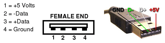
(1+4) Red to Black = 50 Ω - 266 kΩ  The volt meter charging the capacitor is why there is a range.
(1+3) Red to Green = 260 kΩ - 266 kΩ
(1+2) Red to White = 2.5 MΩ
(1+0) Red to Shield = 260 kΩ - 270 kΩ
(3+2) Green to White = 30 kΩ
(3+4) Green to Black = 15 kΩ
(3+0) Green to Shield = 15 kΩ
(2+4) White to Black = 15 kΩ
(2+0) White to Shield = 15 kΩ
(0+4) Shield to Black = 1.3 Ω (would be 0Ω if it wasn't for the USB cable's internal resistance)

[ Attachment Invalid Or Does Not Exist ] 24361[/ATTACH]

The impedance readings that are measured a lot of the time is from other connected circuits that loopback, thus, finding an alternate path between the two test leads.  Think of it as other neighboring circuits looping back and their added resistances sum the meters reading, this is why when testing resistance it is critical to completely isolate the circuit that is to be tested, "ex. lifting one lead of a resistor before measuring it while still connected to the circuit."

Offline bluecar5556

  • Posts: 126
PCB soldering damage
« Reply #28 on: Mon, 15 August 2011, 01:39:18 »
[ Attachment Invalid Or Does Not Exist ] 24371[/ATTACH]

The added wires will be more susceptible to to EMI so try to use as short of path as possible if you must go this route.

Offline Input Nirvana

  • Master of the Calculated Risk
  • Thread Starter
  • Posts: 2316
  • Location: Somewhere in the San Francisco Bay area/Best Coast
  • If I tell ya, I'll hafta kill ya
PCB soldering damage
« Reply #29 on: Mon, 15 August 2011, 16:56:40 »
[ Attachment Invalid Or Does Not Exist ] 24424[/ATTACH]

Gotta hate it when you get 2 different readings from 2 different multimeters on the same setting and on the same connection.

I think I need a third multimeter as a tie breaker.
Kinesis Advantage cut into 2 halves | RollerMouse Free 2 | Apple Magic Trackpad | Colemak
Evil Screaming Flying Door Monkeys From Hell                     Proudly GeekWhacking since 2009
Things change, things stay the same                                        Thanks much, Smallfry  
I AM THE REAPER . . . BECAUSE I KILL IT
~retired from forum activities 2015~

Offline bluecar5556

  • Posts: 126
PCB soldering damage
« Reply #30 on: Mon, 15 August 2011, 17:10:48 »
Touch the leads together on each meter, you should get very close to 0Ω.

Whatever reading you get, subtract that from your final resistance reading.  One meter could have bad test leads or connections.

Offline bluecar5556

  • Posts: 126
PCB soldering damage
« Reply #31 on: Mon, 15 August 2011, 18:23:59 »
[ Attachment Invalid Or Does Not Exist ] 24433[/ATTACH]

D31 Dimension specifications

[ Attachment Invalid Or Does Not Exist ] 24432[/ATTACH] (D31, another alternate wiring schematic)

Parts required:

(2) CM1293: 8-Channel Low Capacitance ESD Protection Diode Array's
(4) 15kΩ resistors, the smallest ones that can be mustered.

Offline Input Nirvana

  • Master of the Calculated Risk
  • Thread Starter
  • Posts: 2316
  • Location: Somewhere in the San Francisco Bay area/Best Coast
  • If I tell ya, I'll hafta kill ya
PCB soldering damage
« Reply #32 on: Mon, 15 August 2011, 18:58:04 »
[ Attachment Invalid Or Does Not Exist ] 24435[/ATTACH]

side by side

leads on the contacts you can see in the ports, measurements of both ports are the same.
Kinesis Advantage cut into 2 halves | RollerMouse Free 2 | Apple Magic Trackpad | Colemak
Evil Screaming Flying Door Monkeys From Hell                     Proudly GeekWhacking since 2009
Things change, things stay the same                                        Thanks much, Smallfry  
I AM THE REAPER . . . BECAUSE I KILL IT
~retired from forum activities 2015~

Offline bluecar5556

  • Posts: 126
PCB soldering damage
« Reply #33 on: Mon, 15 August 2011, 19:04:57 »
Is it possible those USB ports have a slight design differing from the original USB ports?  What i'm getting at is the shield could be protruding in a way that grounds out the signal wires underneath the ports.  Any thing is possible, do you where the USB ports were obtained from?  

The reason I ask is because both USB ports are exhibiting the same problem,  :suspicious:

Offline Input Nirvana

  • Master of the Calculated Risk
  • Thread Starter
  • Posts: 2316
  • Location: Somewhere in the San Francisco Bay area/Best Coast
  • If I tell ya, I'll hafta kill ya
PCB soldering damage
« Reply #34 on: Mon, 15 August 2011, 19:27:49 »
Usb ports came from an ebay seller that has them for different specific laptops, and look like the ones I removed. I don't think there is any issue with the usb ports.

The 1+4, 1+3, 1+2, 1+0 readings are I'm not clear on what range to be using. All the other readings are close to yours.
Kinesis Advantage cut into 2 halves | RollerMouse Free 2 | Apple Magic Trackpad | Colemak
Evil Screaming Flying Door Monkeys From Hell                     Proudly GeekWhacking since 2009
Things change, things stay the same                                        Thanks much, Smallfry  
I AM THE REAPER . . . BECAUSE I KILL IT
~retired from forum activities 2015~

Offline bluecar5556

  • Posts: 126
PCB soldering damage
« Reply #35 on: Tue, 16 August 2011, 00:05:04 »
Locate C474, C478, C1 and C2.  They might be the round electrolytic variety of capacitors.  If you see a line down the side of it, that is the negative lead.  You want to measure continuity (200Ω range) from the lead opposite from the "line," the positive lead to pin 1 (5V) on the USB ports.

[ Attachment Invalid Or Does Not Exist ] 24451[/ATTACH]

Talk to you tomorrow.

Offline Input Nirvana

  • Master of the Calculated Risk
  • Thread Starter
  • Posts: 2316
  • Location: Somewhere in the San Francisco Bay area/Best Coast
  • If I tell ya, I'll hafta kill ya
PCB soldering damage
« Reply #36 on: Tue, 16 August 2011, 12:50:14 »
[ Attachment Invalid Or Does Not Exist ] 24486[/ATTACH]

The solder blog on USB 1 near pin 4 does not have continuity with anything, so it's not causing a short, but it looks like it is.
Kinesis Advantage cut into 2 halves | RollerMouse Free 2 | Apple Magic Trackpad | Colemak
Evil Screaming Flying Door Monkeys From Hell                     Proudly GeekWhacking since 2009
Things change, things stay the same                                        Thanks much, Smallfry  
I AM THE REAPER . . . BECAUSE I KILL IT
~retired from forum activities 2015~

Offline The Solutor

  • Posts: 2262
PCB soldering damage
« Reply #37 on: Tue, 16 August 2011, 13:24:28 »
I've not followed the thread from the start.


Can you briefly summarize ?

What I mean is, usually when an USB port doesen't works it's because is not powered, and when is not powered is because a microfuse is burnt (because a short).

So do you have the 5V line working or not ?
The problem with quotes on the Internet is you never know if they are true  (Abraham Lincoln)

Offline Input Nirvana

  • Master of the Calculated Risk
  • Thread Starter
  • Posts: 2316
  • Location: Somewhere in the San Francisco Bay area/Best Coast
  • If I tell ya, I'll hafta kill ya
PCB soldering damage
« Reply #38 on: Tue, 16 August 2011, 13:41:53 »
There is continuity at pin 1 going back to several components. The mainboard is out, so I don't know if there is actual power being delivered to the pin. I should find a point before a fuse to see if there is continuity. When the laptop was assembled, the device manager saw the posts, but not what was plugged into the ports, and what was plugged in had no indication of power.
Kinesis Advantage cut into 2 halves | RollerMouse Free 2 | Apple Magic Trackpad | Colemak
Evil Screaming Flying Door Monkeys From Hell                     Proudly GeekWhacking since 2009
Things change, things stay the same                                        Thanks much, Smallfry  
I AM THE REAPER . . . BECAUSE I KILL IT
~retired from forum activities 2015~

Offline Input Nirvana

  • Master of the Calculated Risk
  • Thread Starter
  • Posts: 2316
  • Location: Somewhere in the San Francisco Bay area/Best Coast
  • If I tell ya, I'll hafta kill ya
PCB soldering damage
« Reply #39 on: Tue, 16 August 2011, 19:56:33 »
Quote from: bluecar5556;399662
Locate C474, C478, C1 and C2.  They might be the round electrolytic variety of capacitors.  If you see a line down the side of it, that is the negative lead.  You want to measure continuity (200Ω range) from the lead opposite from the "line," the positive lead to pin 1 (5V) on the USB ports.

(Attachment Link) 24451[/ATTACH]

Talk to you tomorrow.

I can only see C478 and C1. No matter which side of those 2 capacitors I'm on, or Pin 1 on either USB port, between the 2 capacitors or the shield or Pin 4, I get the same reading of 2.9.
Kinesis Advantage cut into 2 halves | RollerMouse Free 2 | Apple Magic Trackpad | Colemak
Evil Screaming Flying Door Monkeys From Hell                     Proudly GeekWhacking since 2009
Things change, things stay the same                                        Thanks much, Smallfry  
I AM THE REAPER . . . BECAUSE I KILL IT
~retired from forum activities 2015~

Offline Input Nirvana

  • Master of the Calculated Risk
  • Thread Starter
  • Posts: 2316
  • Location: Somewhere in the San Francisco Bay area/Best Coast
  • If I tell ya, I'll hafta kill ya
PCB soldering damage
« Reply #40 on: Wed, 17 August 2011, 09:56:40 »
I just had a thought! Since both USB ports had been physically damaged (one had all the connectors/pins/plastic completely out of it) is it possible the +5V and GND had shorted before I removed old and replaced with the new USB ports? If only one port is shorted, would it affect both ports? That might make it easier to repair if it is not physical pad/trace damage at the port.

I'm putting the laptop together this morning so I can see if there is power at the port, that seems to be important info.
Kinesis Advantage cut into 2 halves | RollerMouse Free 2 | Apple Magic Trackpad | Colemak
Evil Screaming Flying Door Monkeys From Hell                     Proudly GeekWhacking since 2009
Things change, things stay the same                                        Thanks much, Smallfry  
I AM THE REAPER . . . BECAUSE I KILL IT
~retired from forum activities 2015~

Offline The Solutor

  • Posts: 2262
PCB soldering damage
« Reply #41 on: Wed, 17 August 2011, 10:30:51 »
It's what I'm saying, if the 5V are missing likely both ports are affected, usually there's a single 5v line every two ports.
The problem with quotes on the Internet is you never know if they are true  (Abraham Lincoln)

Offline bluecar5556

  • Posts: 126
PCB soldering damage
« Reply #42 on: Wed, 17 August 2011, 11:39:25 »
Sorry, i've been busy lately.  Can you piece it back together enough to turn the laptop on and still be able to test the polyswitch "U4"?

[ Attachment Invalid Or Does Not Exist ] 24549[/ATTACH]

"The TPS2061 power-distribution switches are intended for applications where heavy capacitive loads and short-circuits are likely to be encountered. This device incorporates 70-m N-channel MOSFET power switches for power-distribution systems that require multiple power switches in a single package. Each switch is controlled by a logic enable input. Gate drive is provided by an internal charge pump designed to control the power-switch rise times and fall times to minimize current surges during switching. The charge pump requires no external components and allows operation from supplies as low as 2.7 V.

When the output load exceeds the current-limit threshold or a short is present, the device limits the output current to a safe level by switching into a constant-current mode, pulling the overcurrent (OCx) logic output low." -Source, TPS2061 Datasheet PDF

[ Attachment Invalid Or Does Not Exist ] 24552[/ATTACH]

Offline bluecar5556

  • Posts: 126
PCB soldering damage
« Reply #43 on: Wed, 17 August 2011, 12:00:18 »
U4 that is depicted by the red arrow in the schematic above looks strikingly similar to what appears to be the chip labelled "U1" on the mainboard, located to the far most left of the image you provided, shown below.

[ Attachment Invalid Or Does Not Exist ] 24553[/ATTACH]

If that is indeed the chip, check for 5V IN @ (pins 2 & 3.)  More importantly, test 5V OUT @ (pins 6, 7 & 8) that terminate to USB1/2 (Pin 1.)

Offline Input Nirvana

  • Master of the Calculated Risk
  • Thread Starter
  • Posts: 2316
  • Location: Somewhere in the San Francisco Bay area/Best Coast
  • If I tell ya, I'll hafta kill ya
PCB soldering damage
« Reply #44 on: Wed, 17 August 2011, 12:01:56 »
U4 is on the reverse side of the mainboard, I will see if I can do that. (I need to re-read the passage to understand exactly what is happening).

Do I check for power coming out of those 3 lines?
Kinesis Advantage cut into 2 halves | RollerMouse Free 2 | Apple Magic Trackpad | Colemak
Evil Screaming Flying Door Monkeys From Hell                     Proudly GeekWhacking since 2009
Things change, things stay the same                                        Thanks much, Smallfry  
I AM THE REAPER . . . BECAUSE I KILL IT
~retired from forum activities 2015~

Offline Input Nirvana

  • Master of the Calculated Risk
  • Thread Starter
  • Posts: 2316
  • Location: Somewhere in the San Francisco Bay area/Best Coast
  • If I tell ya, I'll hafta kill ya
PCB soldering damage
« Reply #45 on: Wed, 17 August 2011, 12:07:31 »
[ Attachment Invalid Or Does Not Exist ] 24554[/ATTACH]
Kinesis Advantage cut into 2 halves | RollerMouse Free 2 | Apple Magic Trackpad | Colemak
Evil Screaming Flying Door Monkeys From Hell                     Proudly GeekWhacking since 2009
Things change, things stay the same                                        Thanks much, Smallfry  
I AM THE REAPER . . . BECAUSE I KILL IT
~retired from forum activities 2015~

Offline bluecar5556

  • Posts: 126
PCB soldering damage
« Reply #46 on: Wed, 17 August 2011, 12:25:56 »
Quote from: input nirvana;400424
Do I check for power coming out of those 3 lines?
Yes, hold one lead to pin 1 (indention mark) GND and test pins 6, 7 & 8 with the other lead, if you read 5V we are in business.  Having a steady hand and preventing the pointed test leads from poking into the solder mask from slipping I can't stress enough.  If there is 5V @ U4 (pins 6, 7 & 8,) check pin 1 for 5V @ USB1&2 and if there is a discrepancy, that is your problem and bridge it with wire after checking for shorts.

Offline Input Nirvana

  • Master of the Calculated Risk
  • Thread Starter
  • Posts: 2316
  • Location: Somewhere in the San Francisco Bay area/Best Coast
  • If I tell ya, I'll hafta kill ya
PCB soldering damage
« Reply #47 on: Wed, 17 August 2011, 12:27:33 »
To power it up to check U4, I need-
 
- power input
- on/off switch
- hard drive
- ram
- lcd screen?
 
Will that do it safely?

Solder mask is a clear coat on the electronics?
Kinesis Advantage cut into 2 halves | RollerMouse Free 2 | Apple Magic Trackpad | Colemak
Evil Screaming Flying Door Monkeys From Hell                     Proudly GeekWhacking since 2009
Things change, things stay the same                                        Thanks much, Smallfry  
I AM THE REAPER . . . BECAUSE I KILL IT
~retired from forum activities 2015~

Offline bluecar5556

  • Posts: 126
PCB soldering damage
« Reply #48 on: Wed, 17 August 2011, 12:38:32 »
you need:

power input
on/off switch
ram

the bios stuck asking for an operating system will suffice, make sure the cpu fan is getting power

Offline Input Nirvana

  • Master of the Calculated Risk
  • Thread Starter
  • Posts: 2316
  • Location: Somewhere in the San Francisco Bay area/Best Coast
  • If I tell ya, I'll hafta kill ya
PCB soldering damage
« Reply #49 on: Wed, 17 August 2011, 12:39:37 »
Got it.

I'm on my way :)
Kinesis Advantage cut into 2 halves | RollerMouse Free 2 | Apple Magic Trackpad | Colemak
Evil Screaming Flying Door Monkeys From Hell                     Proudly GeekWhacking since 2009
Things change, things stay the same                                        Thanks much, Smallfry  
I AM THE REAPER . . . BECAUSE I KILL IT
~retired from forum activities 2015~